Güllü, Hasan Hüseyin
Loading...

Profile URL
Name Variants
Gullu,H.H.
H.,Güllü
H.H.Güllü
G., Hasan Huseyin
Güllü, Hasan Hüseyin
H., Gullu
G.,Hasan Huseyin
H.H.Gullu
Hasan Hüseyin, Güllü
G.,Hasan Hüseyin
Hasan Huseyin, Gullu
Gullu, Hasan Huseyin
Güllü,H.H.
Gullu, H. H.
Gullu, Hasan H.
H.,Güllü
H.H.Güllü
G., Hasan Huseyin
Güllü, Hasan Hüseyin
H., Gullu
G.,Hasan Huseyin
H.H.Gullu
Hasan Hüseyin, Güllü
G.,Hasan Hüseyin
Hasan Huseyin, Gullu
Gullu, Hasan Huseyin
Güllü,H.H.
Gullu, H. H.
Gullu, Hasan H.
Job Title
Doktor Öğretim Üyesi
Email Address
hasan.gullu@atilim.edu.tr
Main Affiliation
Department of Electrical & Electronics Engineering
Status
Former Staff
Website
ORCID ID
Scopus Author ID
Turkish CoHE Profile ID
Google Scholar ID
WoS Researcher ID
Sustainable Development Goals
14
LIFE BELOW WATER

0
Research Products
2
ZERO HUNGER

0
Research Products
11
SUSTAINABLE CITIES AND COMMUNITIES

0
Research Products
1
NO POVERTY

0
Research Products
12
RESPONSIBLE CONSUMPTION AND PRODUCTION

0
Research Products
7
AFFORDABLE AND CLEAN ENERGY

5
Research Products
5
GENDER EQUALITY

0
Research Products
3
GOOD HEALTH AND WELL-BEING

0
Research Products
9
INDUSTRY, INNOVATION AND INFRASTRUCTURE

0
Research Products
13
CLIMATE ACTION

0
Research Products
6
CLEAN WATER AND SANITATION

0
Research Products
10
REDUCED INEQUALITIES

0
Research Products
4
QUALITY EDUCATION

0
Research Products
15
LIFE ON LAND

0
Research Products
16
PEACE, JUSTICE AND STRONG INSTITUTIONS

0
Research Products
17
PARTNERSHIPS FOR THE GOALS

0
Research Products
8
DECENT WORK AND ECONOMIC GROWTH

0
Research Products
This researcher does not have a Scopus ID.
This researcher does not have a WoS ID.
Scholarly Output
55
Articles
52
Views / Downloads
7/0
Supervised MSc Theses
1
Supervised PhD Theses
0
WoS Citation Count
873
Scopus Citation Count
899
WoS h-index
16
Scopus h-index
16
Patents
0
Projects
0
WoS Citations per Publication
15.87
Scopus Citations per Publication
16.35
Open Access Source
8
Supervised Theses
1
Google Analytics Visitor Traffic
| Journal | Count |
|---|---|
| Journal of Materials Science: Materials in Electronics | 16 |
| Physica B: Condensed Matter | 7 |
| Bulletin of Materials Science | 3 |
| Materials Science in Semiconductor Processing | 3 |
| Optik | 3 |
Current Page: 1 / 5
Scopus Quartile Distribution
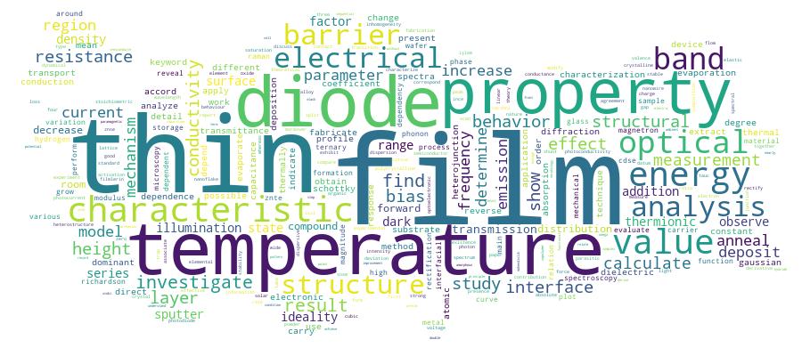
Competency Cloud
29 results
Scholarly Output Search Results
Now showing 1 - 10 of 29
Article Citation - WoS: 9Citation - Scopus: 10Temperature Effects on Optical Characteristics of Cdse Thin Films(Elsevier Sci Ltd, 2021) Gullu, H. H.; Isik, M.; Surucu, O.; Gasanly, N. M.; Parlak, M.CdSe is one of the significant members of II-VI type semiconducting family and it has a wide range of technological applications in which optoelectronic devices take a special position. The present paper reports the structural and optical characteristics of thermally evaporated CdSe thin films. XRD pattern exhibited preferential orientation along (111) plane while atomic composition analyses resulted in the ratio of Cd/Se as closer to 1.0. Temperature-dependent band gap characteristics of CdSe thin films were investigated for the first time by carrying out transmission experiments in the 10-300 K range. The analyses showed that direct band gap energy of the compound decreases from 1.750 (at 10 K) to 1.705 eV (at 300 K). Varshni model was successfully applied to the temperature-band gap energy dependency and various optical constants were determined. Raman spectrum of CdSe thin films was also presented to understand the vibrational characteristics of the compound. The present paper would provide worthwhile data to researchers especially studying on optoelectronic device applications of CdSe thin films.Article Citation - WoS: 11Citation - Scopus: 8Fabrication and Characterization of Tio2 Thin Film for Device Applications(World Scientific Publ Co Pte Ltd, 2019) Hosseini, A.; Gullu, H. H.; Coskun, E.; Parlak, M.; Ercelebi, C.Titanium oxide (TiO2) film was deposited by rectification factor (RF) magnetron sputtering technique on glass substrates and p-Si (111) wafers to fabricate n-TiO2/p-Si heterojunction devices for the investigation of material and device properties, respectively. The structural, surface morphology, optical and electrical properties of TiO(2 )film were characterized by means of scanning electron microscopy (SEM), atomic force microscopy (AFM), X-ray diffraction (XRD), UV-visual (UV-Vis) spectral and dark current-voltage (I-V) measurement analyses. The deposited film layer was found to be homogeneous structure with crack-free surface. The bandgap value of TiO2 film was determined as 3.6 eV and transmission was around 65-85% in the spectral range of 320-1100 nm. The conductivity type of the deposited film was determined as n-type by hot probe method. These values make TiO2 film a suitable candidate as the n-type window layer in possible diode applications. TiO2 film was also deposited on p-Si (111) wafer to obtain Al/n-TiO2/p-Si/Al heterojunction device structure. The dark I-V characteristic was studied to determine the possible conduction mechanisms and diode parameters.Article Citation - WoS: 3Citation - Scopus: 3Fabrication of Cdsexte1-X Thin Films by Sequential Growth Using Double Sources(Elsevier, 2021) Demir, M.; Gullu, H. H.; Terlemezoglu, M.; Parlak, M.CdSexTe(1-x) (CST) ternary thin films were fabricated by stacking thermally evaporated CdSe and electron beam evaporated CdTe layers. The final structure was achieved in a stoichiometric form of approximately Cd:Se:Te = 50:25:25. The post-annealing processes at 300, 400, and 450 degrees C were applied to trigger the compound formation of CST thin films. The X-ray diffraction (XRD) profiles revealed that CdTe and CdSe have major peaks at 23.9 degrees and 25.5 degrees corresponds to (111) direction in cubic zinc-blend structure. Raman modes of CdTe were observed at 140 and 168 cm(-1), while Raman modes of CdSe films were detected at 208 and 417 cm(-1). The post-annealing process was found to be an effective method in order to combine both diffraction peaks and the vibrational modes of CdTe and CdSe, consequently to form CST ternary alloy. Transmission spectroscopy analysis revealed that CST films have direct band gap value of 1.6 eV.Article Citation - WoS: 3Citation - Scopus: 4Analysis of Temperature-Dependent Transmittance Spectra of Zn0.5in0.5< (zis) Thin Films(Springer, 2019) Isik, M.; Gullu, H. H.; Delice, S.; Gasanly, N. M.; Parlak, M.Temperature-dependent transmission experiments of ZnInSe thin films deposited by thermal evaporation method were performed in the spectral range of 550-950nm and in temperature range of 10-300K. Transmission spectra shifted towards higher wavelengths (lower energies) with increasing temperature. Transmission data were analyzed using Tauc relation and derivative spectroscopy. Analysis with Tauc relation was resulted in three different energy levels for the room temperature band gap values of material as 1.594, 1.735 and 1.830eV. The spectrum of first wavelength derivative of transmittance exhibited two maxima positions at 1.632 and 1.814eV and one minima around 1.741eV. The determined energies from both methods were in good agreement with each other. The presence of three band gap energy levels were associated to valence band splitting due to crystal-field and spin-orbit splitting. Temperature dependence of the band gap energies were also analyzed using Varshni relation and gap energy value at absolute zero and the rate of change of gap energy with temperature were determined.Article Citation - WoS: 2Citation - Scopus: 1Investigation of Conductivity Characteristics of Zn-In Thin Films(World Scientific Publ Co Pte Ltd, 2020) Gullu, H. H.; Parlak, M.Zn-In-Se thin films were fabricated on the ultrasonically cleaned glass substrates masked with clover-shaped geometry by thermal evaporation of its elemental sources. Temperature-dependent conductivity characteristics of the films were investigated under dark and illuminated conditions. The semiconductor type of the films was found as n-type by thermal probe test. According to the van der Pauw technique, the dark electrical conductivity analyses showed that the variations of conductivity of unannealed and annealed at 300 degrees C samples are in exponential dependence of temperature. These conductivity profiles were found to be dominated by the thermionic emission at high temperature region whereas their behaviors at low temperatures were modeled by hopping theory. On the contrary, as a result of the further annealing temperatures, the surface of the samples showed semi-metallic characteristics with deviating from expected Arrhenius behavior. In addition, the temperature-dependent photoconductivity of the films was analyzed under different illumination intensities and the results were explained by the supra-linear characteristic based on the two-center recombination model.Conference Object Citation - WoS: 10Citation - Scopus: 10Investigation of Carrier Transport Mechanisms in the Cu-Zn Based Hetero-Structure Grown by Sputtering Technique(Canadian Science Publishing, 2018) Gullu, H. H.; Terlemezoglu, M.; Bayrakli, O.; Yildiz, D. E.; Parlak, M.In this paper, we present results of the electrical characterization of n-Si/p-Cu-Zn-Se hetero-structure. Sputtered film was found in Se-rich behavior with tetragonal polycrystalline nature along with (112) preferred orientation. The band gap energy for direct optical transitions was obtained as 2.65 eV. The results of the conductivity measurements indicated p-type behavior and carrier transport mechanism was modelled according to thermionic emission theory. Detailed electrical characterization of this structure was carried out with the help of temperature-dependent current-voltage measurements in the temperature range of 220-360 K, room temperature, and frequency-dependent capacitance-voltage and conductance-voltage measurements. The anomaly in current-voltage characteristics was related to barrier height inhomogeneity at the interface and modified by the assumption of Gaussian distribution of barrier height, in which mean barrier height and standard deviation at zero bias were found as 2.11 and 0.24 eV, respectively. Moreover, Richardson constant value was determined as 141.95 Acm(-2)K(-2) by means of modified Richardson plot.Article Citation - WoS: 22Citation - Scopus: 24Synthesis and Temperature-Tuned Band Gap Characteristics of Magnetron Sputtered Znte Thin Films(Elsevier, 2020) Isik, M.; Gullu, H. H.; Parlak, M.; Gasanly, N. M.Zinc telluride (ZnTe) is one of the attractive semiconducting compounds used in various optoelectronic devices. The usage of ZnTe in optoelectronic applications directs researchers to search its optical characteristics in great detail. For this purpose, structural and optical properties of magnetron sputtered ZnTe thin films were studied by means of x-ray diffraction and transmission spectroscopy measurements. Structural analyses indicated that ZnTe thin films having cubic crystalline structure were successfully grown on soda-lime glass substrates. Transmittance spectra in the 400-1000 nm were recorded in between 10 and 300 K temperature region. The analyses of absorption coefficient spectra resulted in band gap energies decreasing from around 2.31 (10 K) to 2.26 eV (300 K). Temperature dependency of gap energy was studied by Varshni and O'Donnell-Chen relations to determine various optical parameters like absolute zero temperature band gap energy, change of gap energy with temperature, phonon energy.Article Citation - WoS: 6Citation - Scopus: 7Construction of Self-Assembled Vertical Nanoflakes on Cztsse Thin Films(Iop Publishing Ltd, 2019) Terlemezoglu, M.; Surucu, O. Bayrakli; Colakoglu, T.; Abak, M. K.; Gullu, H. H.; Ercelebi, C.; Parlak, M.Cu2ZnSn(S, Se)(4) (CZTSSe) is a promising alternative absorber material to achieve high power conversion efficiencies, besides its property of involving low-cost and earth-abundant elements when compared to Cu(In, Ga) Se-2 (CIGS) and cadmium telluride (CdTe), to be used in solar cell technology. In this study, a novel fabrication technique was developed by utilizing RF sputtering deposition of CZTSSe thin films having a surface decorated with self-assembled nanoflakes. The formation of nanoflakes was investigated by detailed spectroscopic method of analysis in the effect of each stacked layer deposition in an optimized sequence and the size of nanoflakes by an accurate control of sputtering process including film thickness. Moreover, the effects of substrate temperature on the formation of nanoflakes on the film surface were discussed at a fixed deposition route. One of the main advantages arising from the film surface with self-assembled nanoflakes is the efficient light trapping which decreases the surface reflectance. As a result of the detailed production and characterization studies, it was observed that there was a possibility of repeatable and controllable fabrication sequence for the preparation of CZTSSe thin films with self-textured surfaces yielding low surface reflectance.Article Citation - WoS: 1Citation - Scopus: 1Temperature -Dependent Optical and Electrical Characterization of Cu-Ga Thin Films and Their Diode Characteristics on N-Si(Elsevier Gmbh, 2020) Gullu, H. H.; Isik, M.; Gasanly, N. M.; Parlak, M.In this paper, optical and electrical properties of thermally deposited Cu-Ga-S thin films were investigated using temperature-dependent optical transmission and electrical conductivity measurements. The analysis of the transmission spectra resulted in formation of three direct optical transitions due to the possible valence band splitting in the structure. The band gap values were calculated by means of absorption coefficient and incident photon energy was found in decreasing behavior as the temperature rises. The measured current-voltage values were used to extract the conductivity values which stand in the range of 1.73-2.62 (x104 O-1 cm-1) depending on the ambient temperature. These dark conductivity values were modeled by thermionic emission mechanism. The conductivity activation energies in the structures were calculated as 6.4, 14.5 and 40.7 meV according to the effects of grain boundary potentials. In addition, the films deposited on n-Si wafer showed a diode characteristic under the applied bias voltage between indium (In) front and silver (Ag) back contacts. From current-voltage measurements across the Si-based diode, about four orders of magnitude rectification was observed and the results were analyzed to determine the main diode parameters at dark and room temperature conditions.Article Citation - WoS: 13Citation - Scopus: 15Investigation of electrical characteristics of Ag/ZnO/Si sandwich structure(Springer, 2019) Gullu, H. H.; Surucu, O. Bayrakli; Terlemezoglu, M.; Yildiz, D. E.; Parlak, M.In this study, temperature-dependent current-voltage (I-V), frequency-dependent capacitance-voltage (C-V) and conductance-voltage (G/omega-V) measurements are carried out for the electrical characterization of a zinc oxide (ZnO) thin film-based diode. The sandwich structure in the form of Ag/ZnO/Si/Al is investigated at temperatures between 220 and 360 K and in the frequency region of 1 kHz-1 MHz. ZnO thin film layer is deposited on a p-Si wafer substrate as a transparent conductive oxide layer by taking into consideration possible electronic applications with intrinsic attractive material properties. At each temperature step, the I-V curves showed about two orders of magnitude rectifying behavior and, according to the Schottky diode relation, the saturation current, zero-bias barrier height and ideality factor were extracted as a function of the temperature. In the case of non-ideal diode characteristics due to the inhomogeneties in the diode as observed from the characteristics of the calculated parameters, effective barrier height values are evaluated. In addition, based on the existence of the interface layer, density of interface states in the band gap region and parasitic resistances were determined by the capacitance measurements.

- «
- 1 (current)
- 2
- 3
- »