Sürücü, Özge
Loading...
Profile URL
Name Variants
Bayrakll Ö.
O., Surucu
Bayrakli O.
Bayrakli, Ozge
O.,Surucu
Surucu, Ozge
Ö.,Sürücü
Ozge, Surucu
Sürücü, Özge
Ö., Sürücü
Bayraklı Sürücü Ö.
Özge, Sürücü
Sürücü,Ö.
Surucu, O. Bayrakli
Bayrakli Sürücü O.
Bayraklı Ö.
Surucu,O.
Bayrakli Surucu O.
Bayrakli Ö.
Sürücü Ö.
S.,Ozge
Bayrakli, O.
S., Özge
S., Ozge
S.,Özge
Bayrakli Surucu, Ozge
Surucu O.
Surucu, O.
Bayrakli Sürücü Ö.
Job Title
Doçent Doktor
Email Address
ozge.surucu@atilim.edu.tr
Main Affiliation
Electrical-Electronics Engineering
Status
Website
ORCID ID
Scopus Author ID
Turkish CoHE Profile ID
Google Scholar ID
WoS Researcher ID
Sustainable Development Goals
14
LIFE BELOW WATER

0
Research Products
2
ZERO HUNGER

0
Research Products
11
SUSTAINABLE CITIES AND COMMUNITIES

0
Research Products
1
NO POVERTY

0
Research Products
12
RESPONSIBLE CONSUMPTION AND PRODUCTION

0
Research Products
7
AFFORDABLE AND CLEAN ENERGY

13
Research Products
5
GENDER EQUALITY

0
Research Products
3
GOOD HEALTH AND WELL-BEING

0
Research Products
9
INDUSTRY, INNOVATION AND INFRASTRUCTURE

0
Research Products
13
CLIMATE ACTION

0
Research Products
6
CLEAN WATER AND SANITATION

0
Research Products
10
REDUCED INEQUALITIES

0
Research Products
4
QUALITY EDUCATION

0
Research Products
15
LIFE ON LAND

0
Research Products
16
PEACE, JUSTICE AND STRONG INSTITUTIONS

0
Research Products
17
PARTNERSHIPS FOR THE GOALS

0
Research Products
8
DECENT WORK AND ECONOMIC GROWTH

0
Research Products
This researcher does not have a Scopus ID.
Documents
55
Citations
820
Scholarly Output
44
Articles
41
Views / Downloads
14/0
Supervised MSc Theses
1
Supervised PhD Theses
0
WoS Citation Count
604
Scopus Citation Count
612
WoS h-index
15
Scopus h-index
15
Patents
0
Projects
0
WoS Citations per Publication
13.73
Scopus Citations per Publication
13.91
Open Access Source
5
Supervised Theses
1
Google Analytics Visitor Traffic
| Journal | Count |
|---|---|
| Journal of Materials Science: Materials in Electronics | 7 |
| Applied Physics A | 4 |
| Materials Letters | 3 |
| Materials Science in Semiconductor Processing | 3 |
| Physica Scripta | 3 |
Current Page: 1 / 5
Scopus Quartile Distribution
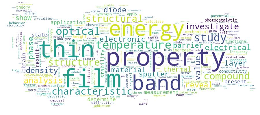
Competency Cloud
35 results
Scholarly Output Search Results
Now showing 1 - 10 of 35
Article Citation - WoS: 6Citation - Scopus: 7Construction of Self-Assembled Vertical Nanoflakes on Cztsse Thin Films(Iop Publishing Ltd, 2019) Terlemezoglu, M.; Surucu, O. Bayrakli; Colakoglu, T.; Abak, M. K.; Gullu, H. H.; Ercelebi, C.; Parlak, M.Cu2ZnSn(S, Se)(4) (CZTSSe) is a promising alternative absorber material to achieve high power conversion efficiencies, besides its property of involving low-cost and earth-abundant elements when compared to Cu(In, Ga) Se-2 (CIGS) and cadmium telluride (CdTe), to be used in solar cell technology. In this study, a novel fabrication technique was developed by utilizing RF sputtering deposition of CZTSSe thin films having a surface decorated with self-assembled nanoflakes. The formation of nanoflakes was investigated by detailed spectroscopic method of analysis in the effect of each stacked layer deposition in an optimized sequence and the size of nanoflakes by an accurate control of sputtering process including film thickness. Moreover, the effects of substrate temperature on the formation of nanoflakes on the film surface were discussed at a fixed deposition route. One of the main advantages arising from the film surface with self-assembled nanoflakes is the efficient light trapping which decreases the surface reflectance. As a result of the detailed production and characterization studies, it was observed that there was a possibility of repeatable and controllable fabrication sequence for the preparation of CZTSSe thin films with self-textured surfaces yielding low surface reflectance.Article Citation - WoS: 11Citation - Scopus: 12Structural and Temperature-Tuned Bandgap Characteristics of Thermally Evaporated β-in2< Thin Films(Springer, 2021) Surucu, O.; Isik, M.; Terlemezoglu, M.; Gasanly, N. M.; Parlak, M.In2S3 is one of the attractive compounds taking remarkable interest in optoelectronic device applications. The present study reports the structural and optical characteristics of thermally evaporated beta-In2S3 thin films. The crystalline structure of the thin films was found as cubic taking into account the observed diffraction peaks in the X-ray diffraction pattern. The atomic compositional ratio of constituent elements was obtained as consistent with chemical formula of In2S3. Three peaks around 275, 309 and 369 cm(-1) were observed in the Raman spectrum. Temperature-tuned bandgap energy characteristics of the In2S3 thin films were revealed from the investigation of transmittance spectra obtained at various temperatures between 10 and 300 K. The analyses of the transmittance spectra indicated that direct bandgap energy of the In2S3 thin films decreases from 2.40 eV (at 10 K) to 2.37 eV (at 300 K) with the increase of measurement temperature. The bandgap energy vs. temperature relation was investigated by means of Varshni optical model. The fitting of the experimental data under the light of theoretical expression revealed the absolute zero bandgap energy, the rate of change of bandgap energy and Debye temperature.Article Citation - WoS: 23Citation - Scopus: 23Exploring Temperature-Dependent Bandgap and Urbach Energies in Cdte Thin Films for Optoelectronic Applications(Elsevier, 2024) Surucu, O.; Surucu, G.; Gasanly, N. M.; Parlak, M.; Isik, M.This study examines CdTe thin films deposited via RF magnetron sputtering, focusing on structural and optical properties. X-ray diffraction, Raman spectroscopy, and SEM assessed structural characteristics. Optical properties were analyzed through transmittance measurements from 10 to 300 K. Tauc plots and Varshni modeling revealed a temperature-dependent bandgap, increasing from 1.49 eV at room temperature to 1.57 eV at 10 K. Urbach energy rose from 82.7 to 93.7 meV with temperature. These results are essential for applications where temperature affects CdTe-based device performance.Conference Object Citation - WoS: 10Citation - Scopus: 10Investigation of Carrier Transport Mechanisms in the Cu-Zn Based Hetero-Structure Grown by Sputtering Technique(Canadian Science Publishing, 2018) Gullu, H. H.; Terlemezoglu, M.; Bayrakli, O.; Yildiz, D. E.; Parlak, M.In this paper, we present results of the electrical characterization of n-Si/p-Cu-Zn-Se hetero-structure. Sputtered film was found in Se-rich behavior with tetragonal polycrystalline nature along with (112) preferred orientation. The band gap energy for direct optical transitions was obtained as 2.65 eV. The results of the conductivity measurements indicated p-type behavior and carrier transport mechanism was modelled according to thermionic emission theory. Detailed electrical characterization of this structure was carried out with the help of temperature-dependent current-voltage measurements in the temperature range of 220-360 K, room temperature, and frequency-dependent capacitance-voltage and conductance-voltage measurements. The anomaly in current-voltage characteristics was related to barrier height inhomogeneity at the interface and modified by the assumption of Gaussian distribution of barrier height, in which mean barrier height and standard deviation at zero bias were found as 2.11 and 0.24 eV, respectively. Moreover, Richardson constant value was determined as 141.95 Acm(-2)K(-2) by means of modified Richardson plot.Article Citation - WoS: 8Citation - Scopus: 8Complex Nodal Structure Phonons Formed by Open and Closed Nodal Lines in Coass and Na2cup Solids(Royal Soc Chemistry, 2022) Ding, Guangqian; Sun, Tingting; Surucu, Gokhan; Surucu, Ozge; Gencer, Aysenur; Wang, XiaotianTopological phononic states with nodal lines not only have updated our knowledge of the phases of matter in a fundamental way, but also have become a major frontier research direction in condensed matter physics. From a mathematical perspective, nodal line phonons can be divided into open and closed types. The present attempt is a report on the coexistence of such open and closed nodal line phonons in two realistic solids, CoAsS and Na2CuP, based on first-principles calculations. Furthermore, it is shown that the closed and the open nodal line states in CoAsS and Na2CuP have touching points and can form a complex nodal structure phonon in a momentum space. Due to the topologically non-trivial behavior of the complex nodal structure in both phonons, evident phononic surface states occur in the projected surfaces of both materials. In this way, these states, arising from the projected crossing points, can benefit experimental detection in follow-up studies. It has been stated that the open and closed nodal line states are formed by the crossings of two phonon branches and, hence, these two types of nodal line phonons are coupled with each other. The results obtained here could be considered as a breakthrough in clearly demonstrating the coexistence of the open and closed nodal line states in phonons and, for this reason, may inspire researchers seeking materials with such topological states in other bosons, such as photons.Article Citation - WoS: 9Citation - Scopus: 9Temperature Effects on Optical Characteristics of Thermally Evaporated Cusbse2 Thin Films for Solar Cell Applications(Elsevier, 2022) Surucu, O.; Isik, M.; Terlemezoglu, M.; Bektas, T.; Gasanly, N. M.; Parlak, M.CuSbSe2 thin film was deposited by co-evaporation of binary CuSe and Sb2Se3 sources. The structural and morphological properties of the deposited thin film were investigated with X-ray diffraction (XRD), scanning electron microscopy (SEM), and energy-dispersive X-ray analysis measurements. XRD pattern indicated that deposited thin film has an orthorhombic crystalline structure with the preferential orientation of (013) direction. SEM image presented that the thin film surface is almost uniform. The optical characteristics of the deposited CuSbSe2 thin film were investigated in detail by performing room temperature Raman, temperature-dependent transmittance spectroscopy, and photoluminescence techniques. Raman spectrum exhibited one mode at around 210 cm(-1) associated with A(g) vibrational mode. The derivative spectroscopy technique was used to obtain the band gap energy of the films. Temperature dependence of band gap energy was investigated by considering the Varshni model. The rate of change of band gap energy, absolute zero value of gap energy, and Debye temperature were determined as 1.3 x 10(-4) eV/K, 1.21 eV, and 297 +/- 51 K, respectively. The photoluminescence spectrum indicated the room temperature direct band gap energy as 1.30 eV.Article Citation - WoS: 2Citation - Scopus: 2Performance Enhancement of Silicon Photodiodes Through the Integration of Green Synthesized Reduced Graphene Oxide Variants(Iop Publishing Ltd, 2024) Yildiz, D. E.; Sürücü, Özge; Surucu, O.; Balaban, H. Mert; Bilici, I; Yildirim, M.; Sürücü, Özge; Electrical-Electronics Engineering; Electrical-Electronics EngineeringThis study examines the potential of enhancing the optoelectronic properties of silicon photodiodes by producing and analyzing heterostructures that incorporate reduced graphene oxide (rGO) synthesized with silicon using different reduction methods. Graphene oxide (GO) was manufactured utilizing an enhanced Hummers' method. Subsequently, reduced graphene oxides (rGOs) were made by chemical and thermal reduction processes, which are considered ecologically friendly. The use of ascorbic acid to produce ascorbic acid-reduced graphene oxide (ArGO) and thermal processing to produce thermally reduced graphene oxide (TrGO) have significantly contributed to the development of high-performance photodiode technology. The electrical properties were carefully assessed under different levels of light, revealing the substantial impact of integrating reduced graphene oxides (rGOs) on the performance of the diodes. Comparing ArGO/Si, TrGO/Si, and GO/Si heterostructures shows that customized rGO has the potential to greatly influence the responsivity and efficiency of Si-based optoelectronic devices, making a significant contribution to photodiode technology.Article Citation - WoS: 1Deposition and Characterization of ZnSnSe2 Thin-Films Deposited by Using Sintered Stoichiometric Powder(Gazi Univ, 2019) Bayrakli Surucu, Ozge; Gullu, Hasan HuseyinIn this work, ZnSnSe2 (ZTSe) thin films were deposited using crystalline powder grown by vertical Bridgman-Stockbarger technique. The deposition process was carried out by means of e-beam evaporation on the well-cleaned soda lime glass substrates and keeping them at the substrate temperature of 200 degrees C. The structural, optical and electrical properties of ternary ZTSe thin films were investigated depending on the annealing temperature at 250 and 300 degrees C. X-ray diffraction analysis showed that as-grown films were in amorphous structure, however annealing at 250 degrees C triggered the crystallization on the preferred ternary structure and annealing at 300 degrees C resulted in the changes from amorphous to the polycrystalline structure. Using the compositional analysis, the detail information about the stoichiometry and the segregation mechanisms of the constituent elements in the structure were determined for both as-grown and annealed samples. In addition, they were morphologically characterized using scanning electron microscopy technique. The electrical properties were analyzed using temperature dependent dark- and photo-conductivity measurements. From the variation of electrical conductivity as a function of the ambient temperature, the current transport mechanisms and corresponding activation energies at specific temperature intervals for each sample were determined. The optical properties for the ZTSe thin films were studied depending on the structural changes with annealing.Article Citation - WoS: 5Citation - Scopus: 5Physical Characterization of Thermally Evaporated Sn-Sb Thin Films for Solar Cell Applications(Springer Heidelberg, 2023) Bektas, Tunc; Surucu, Ozge; Terlemezoglu, Makbule; Parlak, MehmetThe substitution of Sb in binary SnSe structure may lead to tailoring the physical properties of both SnSe and SbSe, promising absorber layers for thin film solar cells. The resulting Sn-Sb-Se structure could be an outstanding material for photovoltaic applications. In this study, Sn-Sb-Se thin films were deposited by thermal evaporation, and the effect of annealing on the films' structural, optical, and electrical properties were reported. XRD measurement shows that annealing at 300 degrees C yields the best crystalline quality, and structural parameters were calculated using XRD data. SEM and AFM measurements indicate deformation in the film surface after annealing at 400 degrees C. UV-Vis spectroscopy measurement provides a high absorption coefficient which indicates a direct band gap. The band gap and activation energies of the as-grown sample were found as 1.59 eV and 106.1 meV, respectively. The results of SEM, AFM, XRD, Raman, UV-Vis spectroscopy and temperature-dependent photoconductivity measurements were discussed throughout the paper.Article Citation - WoS: 4Citation - Scopus: 4Growth and Optical Characterization of Sn0.6sb0.4< Layer Single Crystals for Optoelectronic Applications(Elsevier Sci Ltd, 2022) Bektas, T.; Terlemezoglu, M.; Surucu, O.; Isik, M.; Parlak, M.SnSe compound is an attractive semiconductor material due to its usage in photovoltaic applications. The sub-stitution of Sb in the SnSe compound presents a remarkable advantage especially in point of tuning optical characteristics. The present paper reports the structural and optical properties of Sn1-xSbxSe (x = 0.4) layered single crystals grown by the vertical Bridgman method. To the best of our knowledge, this work is the first investigation of the Sn0.6Sb0.4Se crystal grown with the vertical Bridgman technique. X-ray diffraction (XRD) pattern of the grown crystal indicated the well crystalline structure of the grown crystals. Lattice strain and interplanar spacing of the crystal structure were determined using the XRD pattern. Scanning electron micro-scope images allowed to the observation of the layer crystal structure. The layer crystalline structure shows 2D material properties and provides 2D applications. Optical properties were revealed by carrying out Raman, ellipsometry and transmission measurements. Raman modes, refractive index, extinction coefficient, and dielectric spectra, band gap energy of the crystal were presented throughout the paper. The obtained results indicated that Sn1-xSbxSe (x = 0.4) layer single crystals may be an alternative potential for photovoltaic and optoelectronic applications.
