Sürücü, Özge
Loading...
Profile URL
Name Variants
Bayrakll Ö.
O., Surucu
Bayrakli O.
Bayrakli, Ozge
O.,Surucu
Surucu, Ozge
Ö.,Sürücü
Ozge, Surucu
Sürücü, Özge
Ö., Sürücü
Bayraklı Sürücü Ö.
Özge, Sürücü
Sürücü,Ö.
Surucu, O. Bayrakli
Bayrakli Sürücü O.
Bayraklı Ö.
Surucu,O.
Bayrakli Surucu O.
Bayrakli Ö.
Sürücü Ö.
S.,Ozge
Bayrakli, O.
S., Özge
S., Ozge
S.,Özge
Bayrakli Surucu, Ozge
Surucu O.
Surucu, O.
Bayrakli Sürücü Ö.
Job Title
Doçent Doktor
Email Address
ozge.surucu@atilim.edu.tr
Main Affiliation
Electrical-Electronics Engineering
Status
Website
ORCID ID
Scopus Author ID
Turkish CoHE Profile ID
Google Scholar ID
WoS Researcher ID
Sustainable Development Goals
14
LIFE BELOW WATER

0
Research Products
2
ZERO HUNGER

0
Research Products
11
SUSTAINABLE CITIES AND COMMUNITIES

0
Research Products
1
NO POVERTY

0
Research Products
12
RESPONSIBLE CONSUMPTION AND PRODUCTION

0
Research Products
7
AFFORDABLE AND CLEAN ENERGY

13
Research Products
5
GENDER EQUALITY

0
Research Products
3
GOOD HEALTH AND WELL-BEING

0
Research Products
9
INDUSTRY, INNOVATION AND INFRASTRUCTURE

0
Research Products
13
CLIMATE ACTION

0
Research Products
6
CLEAN WATER AND SANITATION

0
Research Products
10
REDUCED INEQUALITIES

0
Research Products
4
QUALITY EDUCATION

0
Research Products
15
LIFE ON LAND

0
Research Products
16
PEACE, JUSTICE AND STRONG INSTITUTIONS

0
Research Products
17
PARTNERSHIPS FOR THE GOALS

0
Research Products
8
DECENT WORK AND ECONOMIC GROWTH

0
Research Products
This researcher does not have a Scopus ID.
Documents
55
Citations
826
Scholarly Output
44
Articles
41
Views / Downloads
14/0
Supervised MSc Theses
1
Supervised PhD Theses
0
WoS Citation Count
608
Scopus Citation Count
613
WoS h-index
15
Scopus h-index
15
Patents
0
Projects
0
WoS Citations per Publication
13.82
Scopus Citations per Publication
13.93
Open Access Source
5
Supervised Theses
1
Google Analytics Visitor Traffic
| Journal | Count |
|---|---|
| Journal of Materials Science: Materials in Electronics | 7 |
| Applied Physics A | 4 |
| Materials Letters | 3 |
| Materials Science in Semiconductor Processing | 3 |
| Physica Scripta | 3 |
Current Page: 1 / 5
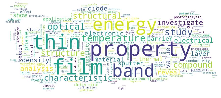
Competency Cloud