Qasrawı, Atef Fayez Hasan

Loading...
Profile Picture
Name Variants
Qasrawi, Atef Fayez
Atef Fayez Hasan, Qasrawı
Qasrawı,A.F.H.
Qasrawi,A.F.H.
Q., Atef Fayez Hasan
Q.,Atef Fayez Hasan
Atef Fayez Hasan, Qasrawi
Qasrawi, Atef Fayez Hasan
A.F.H.Qasrawı
A.F.H.Qasrawi
A., Qasrawi
A.,Qasrawı
Qasrawı, Atef Fayez Hasan
Qasrawi, A. F.
Qasrawi,A.F.
Qasrawi, AF
Qasrawi, Atef F.
Qasrawi, Atef A.
Qasrawi, Atef Fayez
Qasrawi, Atef F.
Qasrawi, Atef A.
Qasrawi, Atef
Job Title
Doçent Doktor
Email Address
atef.qasrawi@atilim.edu.tr
Main Affiliation
Department of Electrical & Electronics Engineering
Status
Former Staff
Website
ORCID ID
Scopus Author ID
Turkish CoHE Profile ID
Google Scholar ID
WoS Researcher ID

Sustainable Development Goals

2

ZERO HUNGER
ZERO HUNGER Logo

0

Research Products

11

SUSTAINABLE CITIES AND COMMUNITIES
SUSTAINABLE CITIES AND COMMUNITIES Logo

0

Research Products

14

LIFE BELOW WATER
LIFE BELOW WATER Logo

0

Research Products

6

CLEAN WATER AND SANITATION
CLEAN WATER AND SANITATION Logo

0

Research Products

1

NO POVERTY
NO POVERTY Logo

0

Research Products

5

GENDER EQUALITY
GENDER EQUALITY Logo

0

Research Products

9

INDUSTRY, INNOVATION AND INFRASTRUCTURE
INDUSTRY, INNOVATION AND INFRASTRUCTURE Logo

0

Research Products

16

PEACE, JUSTICE AND STRONG INSTITUTIONS
PEACE, JUSTICE AND STRONG INSTITUTIONS Logo

1

Research Products

17

PARTNERSHIPS FOR THE GOALS
PARTNERSHIPS FOR THE GOALS Logo

0

Research Products

15

LIFE ON LAND
LIFE ON LAND Logo

0

Research Products

10

REDUCED INEQUALITIES
REDUCED INEQUALITIES Logo

0

Research Products

7

AFFORDABLE AND CLEAN ENERGY
AFFORDABLE AND CLEAN ENERGY Logo

17

Research Products

8

DECENT WORK AND ECONOMIC GROWTH
DECENT WORK AND ECONOMIC GROWTH Logo

0

Research Products

4

QUALITY EDUCATION
QUALITY EDUCATION Logo

0

Research Products

12

RESPONSIBLE CONSUMPTION AND PRODUCTION
RESPONSIBLE CONSUMPTION AND PRODUCTION Logo

0

Research Products

3

GOOD HEALTH AND WELL-BEING
GOOD HEALTH AND WELL-BEING Logo

0

Research Products

13

CLIMATE ACTION
CLIMATE ACTION Logo

0

Research Products
This researcher does not have a Scopus ID.
This researcher does not have a WoS ID.
Scholarly Output

222

Articles

218

Views / Downloads

642/0

Supervised MSc Theses

0

Supervised PhD Theses

0

WoS Citation Count

1887

Scopus Citation Count

1907

WoS h-index

21

Scopus h-index

21

Patents

0

Projects

0

WoS Citations per Publication

8.50

Scopus Citations per Publication

8.59

Open Access Source

17

Supervised Theses

0

Google Analytics Visitor Traffic

JournalCount
Journal of Electronic Materials15
Crystal Research and Technology13
physica status solidi (a)12
Journal of Alloys and Compounds11
Materials Science in Semiconductor Processing11
Current Page: 1 / 11

Scopus Quartile Distribution

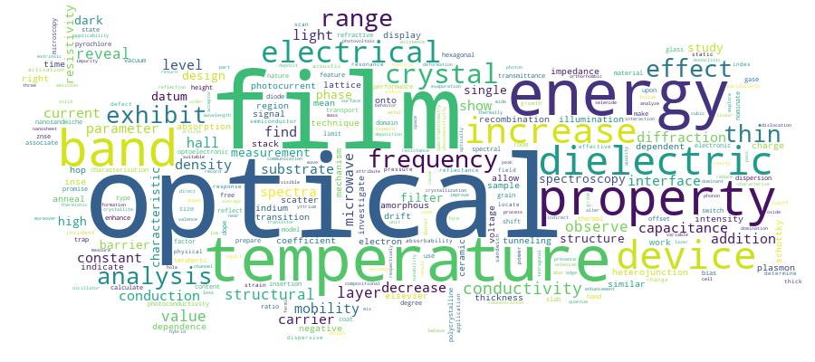
Competency Cloud

GCRIS Competency Cloud

Scholarly Output Search Results

Now showing 1 - 6 of 6
  • Article
    Citation - WoS: 18
    Citation - Scopus: 18
    Fabrication of Al/Mgo and C/Mgo Tunneling Barriers for Tunable Negative Resistance and Negative Capacitance Applications
    (Elsevier Science Bv, 2013) Qasrawi, A. F.
    In this work, the design and characterization of magnesium oxide based tunneling diodes which are produced on Al and InSe films as rectifying substrates are investigated. It was found that when Al thin films are used, the device exhibit tunneling diode behavior of sharp valley at 0.15 V and peak to valley current ratio (PVCR) of 11.4. In addition, the capacitance spectra of the Al/MgO/C device show a resonance peak of negative capacitance (NC) values at 44.7 MHz. The capacitance and resistance-voltage characteristics handled at an ac signal frequency of 100 MHz reflected a build in voltage (V-bi) of 1.29 V and a negative resistance (NR) effect above 2.05 V. This device quality factor (Q)-voltage response is similar to 10(4). When the Al substrate is replaced by InSe thin film, the tunneling diode valley appeared at 1.1 V. In addition, the PVCR, NR range, NC resonance peak, Q and lib; are found to be 135, 0.94-2.24 and 39.0 MHz, similar to 10(5) and 1.34 V, respectively. Due to the wide differential negative resistance and capacitance voltage ranges and due to the response of the C/MgO/InSe/C device at 1.0 GHz, these devices appear to be suitable for applications as frequency mixers, amplifiers, and monostable-bistable circuit elements (MOBILE). (c) 2013 Elsevier B.V. All rights reserved.
  • Article
    Citation - WoS: 18
    Citation - Scopus: 18
    Heat Treatment Effects on the Structural and Electrical Properties of Thermally Deposited Agin5s8< Thin Films
    (Pergamon-elsevier Science Ltd, 2011) Qasrawi, A. F.; Kayed, T. S.; Ercan, Filiz
    The heat treatment effects on structural and electrical properties of thermally deposited AgIn5S8 thin films have been investigated. By increasing the annealing temperature of the sample from 450 to 500 K, we observed a change in the crystallization direction from (420) to (311). Further annealing of the AgIn5S8 films at 550, 600 and 650 K resulted in larger grain size in the (311) preferred direction. The room temperature electrical resistivity, Hall coefficient and Hall mobility were significantly influenced by higher annealing temperatures. Three impurity levels at 230, 150, and 78 meV were detected for samples annealed at 350 K. The electrical resistivity decreased by four orders of magnitude when the sample annealing temperature was raised from 350 to 450 K. The temperature dependent electrical resistivity and carrier concentration of the thin film samples were studied in the temperature ranges of 25-300 K and 140-300 K, respectively. A degenerate-nondegenerate semiconductor transition at approximately 180 was observed for samples annealed at 450 and 500 K. Similar type of transition was observed at 240 K for samples annealed at 600 and 650 K. (C) 2011 Elsevier Ltd. All rights reserved.
  • Article
    Citation - WoS: 7
    Citation - Scopus: 7
    Photoconductivity Kinetics in Agin5s8< Thin Films
    (Elsevier Science Sa, 2010) Qasrawi, A. F.; Kayed, T. S.; Ercan, Ismail
    The temperature (T) and illumination intensity (F) effects on the photoconductivity of as grown and heat-treated AgIn5S8 thin films has been investigated. At fixed illumination intensity, in the temperature region of 40-300K, the photocurrent (I-ph) of the films was observed to decrease with decreasing temperature. The I-ph of the as grown sample behaved abnormally in the temperature region of 170-180K. At fixed temperature and variable illumination intensity, the photocurrent of the as grown sample exhibited linear, sublinear and supralinear recombination mechanisms at 300 K and in the regions of 160-260K and 25-130 K. respectively. This behavior is attributed to the exchange of role between the linear recombination at the surface near room temperature and trapping centers in the film which become dominant as temperature decreases. Annealing the sample at 350 K for 1 h improved the characteristic curves of I-ph. The abnormality disappeared and the I-ph - T dependence is systematic. The data analysis of which revealed two recombination centers located at 66 and 16 meV. In addition, the sublinear recombination mechanism disappeared and the heat-treated films exhibited supralinear recombination in most of the studied temperature range. (C) 2010 Elsevier B.V. All rights reserved.
  • Article
    Citation - WoS: 10
    Citation - Scopus: 10
    Temperature effects on the optoelectronic properties of AgIn5S8 thin films
    (Elsevier Science Sa, 2011) Qasrawi, A. F.
    Polycrystalline AgIn5S8 thin films are obtained by the thermal evaporation of AgIn5S8 crystals onto ultrasonically cleaned glass substrates under a pressure of similar to 1.3 x 10(-3) Pa. The temperature dependence of the optical band gap and photoconductivity of these films was studied in the temperature regions of 300-450 K and 40-300 K, respectively. The heat treatment effect at annealing temperatures of 350, 450 and 550 K on the temperature dependent photoconductivity is also investigated. The absorption coefficient, which was studied in the incidence photon energy range of 1.65-2.55 eV, increased with increasing temperature. Consistently, the absorption edge shifts to lower energy values as temperature increases. The fundamental absorption edge which corresponds to a direct allowed transition energy band gap of 1.78 eV exhibited a temperature coefficient of -3.56 x 10(-4) eV/K. The 0 K energy band gap is estimated as 1.89 eV. AgIn5S8 films are observed to be photoconductive. The highest and most stable temperature invariant photocurrent was obtained at an annealing temperature of 550 K. The photoconductivity kinetics was attributed to the structural modifications caused by annealing and due to the trapping-recombination centers' exchange. (C) 2010 Elsevier B.V. All rights reserved.
  • Article
    Citation - WoS: 10
    Citation - Scopus: 9
    Tunable Au/Ga2< Varactor Diodes Designed for High Frequency Applications
    (Natl inst R&d Materials Physics, 2017) Al Garni, S. E.; Qasrawi, A. F.; Department of Electrical & Electronics Engineering
    In this work, the design and characterization of Au/Ga2S3/Yb Schottky barrier is investigated by means of transmittance electron microscopy (TEM), scanning electron microscopy (SEM), energy dispersive X-ray spectroscopy (EDXS), capacitance spectroscopy, capacitance (C)-voltage (V) characteristics and impedance spectroscopy techniques. The design of the energy band diagram of the amorphous Au/Ga2S3 interface revealed a theoretical energy barrier height (q phi(b)) and built in voltage (qV(bi)) of 2.04 and 1.88 eV, respectively. Experimentally, the qV(bi) was observed to be sensitive to the applied signal frequency. In addition, the capacitance spectra which were studied in the range of 10-1800 MHz, revealed resonance and antiresonance biasing dependent signal oscillations associated with negative capacitance values. On the other hand, impedance spectroscopy analysis revealed band pass/reject filtering properties in all the studied frequency range. The device exhibited a return loss, voltage standing wave ratio and power efficiency of 16.7 dB, 1.3 and 98.3% at 1400 MHz, respectively.
  • Article
    Citation - WoS: 10
    Citation - Scopus: 10
    Light Intensity Effects on Electrical Properties of Agin5s8< Thin Films
    (Elsevier Science Sa, 2011) Qasrawi, A. F.
    The light illumination effects on the current conduction mechanism in thermally annealed polycrystalline AgIn5S8 thin films has been investigated by means of dark and photoexcited conductivity measurements as a function of temperature. The dark electrical conductivity analysis in the temperature region of 30-300 K, reflected the domination of thermionic emission and variable range hopping of charge carriers over the grain boundaries above and below 90 K, respectively. Conductivity activation energies of similar to 155 and 78 meV (in the temperature regions of 230-300 K and 90-220 K. respectively), a density of localized states (evaluated assuming a localization length of 5A(0)) of 1.17 x 10(20) cm(-3) eV(-1), an average hopping distance of 41.51 A(0) (at 60 K) and an average hopping energy of 28.64 meV have been determined from the dark electrical measurements. When the sample was exposed to illumination at specific excitation intensity, the values of the conductivity activation energy, the average hopping energy and the average hopping range were decreased significantly. On the other hand, the density of localized states near the Fermi level increased when the light intensity was increased. Such behavior is attributed to the temporary shift in Fermi level and/or trap density reduction by electron-hole recombination. (C) 2011 Elsevier B.V. All rights reserved.